Company & Professionals
OiTec Oy
Since 2013, our company has experienced a steady economical growth which we strive to maintain
-
Founded 2013
-
2021 Turnover 4M€
-
2022 Turnover 5.9M€
-
2023 Turnover estimation 9,5M€
-
2024 Turnover target 12M€ Subtext
Our office and manufacturing facilities are located in Jorvas HighTech Center in Kirkkonummi, just 30 km outside of Helsinki. The address is:
Hirsalantie 11
FI-02420 Jorvas
Finland
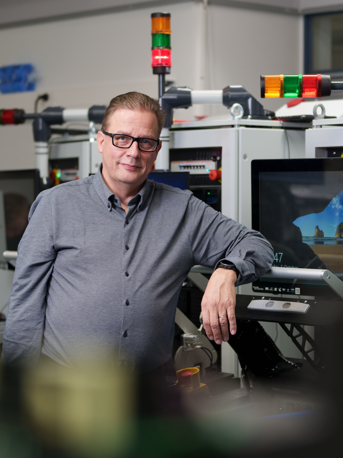
Pekka Oinonen, CEO
Contact: firstname.lastname@oitec.fi
OiTec employs the best professionals in the field to ensure comprehensive high-quality testing protocols
-
+5 Project Managers to manage projects
-
+40 Designers to design high end test systems
-
+5 Assemblers to manufacture high end test systems
-
Wide partner network
-
HW Design Engineering (PADS, EPLAN)
-
Test SW Design Engineering (LabVIEW, TestStand, Boundary Scan with JTAG & Göpel)
-
Mechanical Design Engineering (CREO, SolidWorks, AUTOCAD)
-
Layout Design (PADS)
-
Project Management (Severa, MS Project)
-
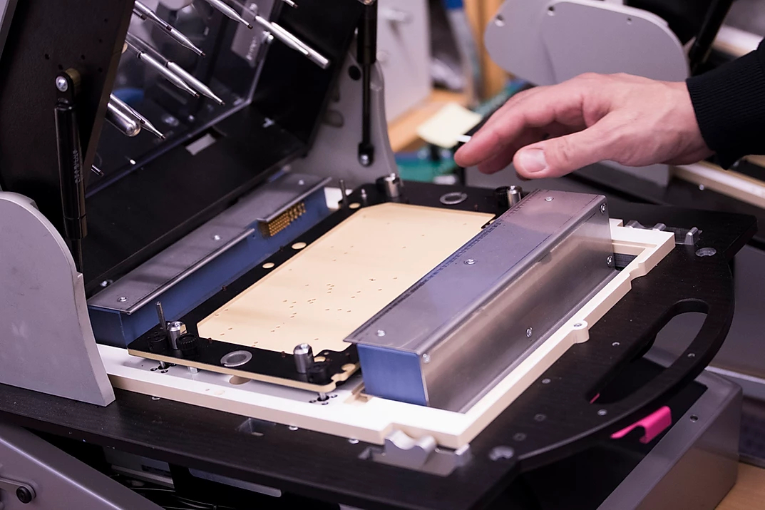
New ESD Shielded areas for assembly and testing
All employees have completed electrical safety training and are issued occupational safety card for a 4-hour emergency training.
Design partners
-
Vinditec Oy
-
SalDigi Oy
-
PLE-Mechanics
-
Cadmic Oy